TinyComputer TD4
FPGAに、小さなコンピュータのTD4を入れてみました。 その内容を記します。
作成動機
「CPUの創りかた」という本は、発売された頃に 読んで知っていました。実際に作るには、部品代が嵩むし、半田付けの時間が 取れないので敬遠していました。 所要でホームタウン内を歩いていると、大学の非常勤講師を していた頃の教え子に会ったので、喫茶店で近況などを話し ていました。 話題がデジタル回路になり、「CPUの創りかた」で公開されて いるCPUのTD4を、PLDで簡単に作れますかと質問が出ました。 「簡単だろうなあ。」と返答すると、「新人教育用に、VHDL コードを書いてくれますか。」ときました。 「雀の涙程度の予算なので、夕食3回分で如何でしょう。」と 畳掛けるので、こちらが作るなら、XilinxのFPGAを使うことを 条件にすると、それでよいと。 それならばと、OKしました。 ここまでが、作成に至る経緯と動機です。
システム設計
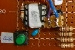
TD4の仕様と見直すと、CPUの回路自体は単純なのですが ROMに相当する部分は、簡単に内容を変えられるように した方が、教育には使いやすくなると判断しました。 どう実現するかを少し考え、次の結論に到達しました。 ROMに相当するメモリの容量は、16バイト。 4入力8出力のデコーダがROMで実現できればよい。 デコーダは単純な組み合わせ回路なので、それだけ は、毎回定義する。 内部ブロックは、次のようにします。ROMの中に入れる8ビットの16バイト情報は、PC上の スクリプト言語で作ることに。これがアセンブラに なります。 使えるスクリプト言語は、AWK、Tcl/Tk、Pythonですが アセンブラでよいので、AWKで作りました。 スクリプトコードは、以下。 BEGIN { printf("TD4 assembler\n"); printf(" adr data ------------------------\n"); } { # get code instructionx = tolower($1) oprandx = tolower($2) # split idx = index(oprandx,",") if ( idx == 0 ) { oprand0 = oprandx } else { oprand0 = substr(oprandx,idx-1,1) oprand1 = substr(oprandx,idx+1,2) } # conversion opcode = 15 oprand = 15 # add if ( instructionx == "add" ) { oprand = oprand1 if ( oprand0 == "a" ) { opcode = 0 } if ( oprand0 == "b" ) { opcode = 5 } } # mov if ( instructionx == "mov" ) { oprand = oprand1 if ( oprand0 == "a" ) { opcode = 3 oprand = oprand1 if ( oprand1 == "b" ) { opcode = 1 oprand = 0 } } if ( oprand0 == "b" ) { opcode = 7 oprand = oprand1 if ( oprand1 == "a" ) { opcode = 4 oprand = 0 } } } # in if ( instructionx == "in" ) { oprand = 0 if ( idx != 0 ) { # default oprand = oprand1 # hexadecimal if ( oprand1 == "a" ) { oprand = 10 } if ( oprand1 == "b" ) { oprand = 11 } if ( oprand1 == "c" ) { oprand = 12 } if ( oprand1 == "d" ) { oprand = 13 } if ( oprand1 == "e" ) { oprand = 14 } if ( oprand1 == "f" ) { oprand = 15 } } if ( oprand0 == "a" ) { opcode = 2 } if ( oprand0 == "b" ) { opcode = 6 } } # out if ( instructionx == "out" ) { oprand = 0 if ( idx != 0 ) { # default oprand = oprand1 # hexadecimal if ( oprand1 == "a" ) { oprand = 10 } if ( oprand1 == "b" ) { oprand = 11 } if ( oprand1 == "c" ) { oprand = 12 } if ( oprand1 == "d" ) { oprand = 13 } if ( oprand1 == "e" ) { oprand = 14 } if ( oprand1 == "f" ) { oprand = 15 } } opcode = 11 if ( oprand0 == "b" ) { opcode = 9 } } # JNC if ( instructionx == "jnc" ) { opcode = 14 oprand = oprand0 } # JMP if ( instructionx == "jmp" ) { opcode = 15 oprand = oprand0 } # generate code result = opcode * 16 + oprand # show printf(" 0x%02X 0x%02X => %s\n",NR-1,result,$0) } END { printf("---------------------------------------\n"); } テキストファイルにニモニックでプログラムを 作成し、AWKで変換します。 c:\>gawk -f td4asm.awk test.txt > tout.txt I/Oリダイレクトでテキストファイルにすると以下となります。 TD4 assembler adr data ------------------------ 0x00 0x30 => MOV A,0 0x01 0x01 => ADD A,1 0x02 0x4A => MOV B,A 0x03 0x90 => OUT B 0x04 0xF1 => JMP 1 --------------------------------------- ROMに入力するデコーダ情報がわかったので、VHDLコードを 定義します。 library IEEE; use IEEE.STD_LOGIC_1164.ALL; use IEEE.STD_LOGIC_ARITH.ALL; use IEEE.STD_LOGIC_UNSIGNED.ALL; entity tdrom is port ( -- address input XADR : in std_logic_vector(3 downto 0) ; -- ROM output XDout : out std_logic_vector(7 downto 0) -- ; ) ; end tdrom ; architecture Behavioral of tdrom is -- input signal iXADR : std_logic_vector(3 downto 0) ; -- output signal iDout : std_logic_vector(7 downto 0) ; begin -- input iXADR <= XADR ; -- output XDout <= iDout ; -- decode iDout <= X"30" when ( iXADR = "0000" ) else -- MOV A,0 X"01" when ( iXADR = "0001" ) else -- ADD A,1 X"40" when ( iXADR = "0010" ) else -- MOV B,A X"90" when ( iXADR = "0011" ) else -- OUT B X"F1" when ( iXADR = "0100" ) else -- JMP 1 X"FF" when ( iXADR = "0101" ) else -- JMP 15 X"FF" when ( iXADR = "0110" ) else -- JMP 15 X"FF" when ( iXADR = "0111" ) else -- JMP 15 X"FF" when ( iXADR = "1000" ) else -- JMP 15 X"FF" when ( iXADR = "1001" ) else -- JMP 15 X"FF" when ( iXADR = "1010" ) else -- JMP 15 X"FF" when ( iXADR = "1011" ) else -- JMP 15 X"FF" when ( iXADR = "1100" ) else -- JMP 15 X"FF" when ( iXADR = "1101" ) else -- JMP 15 X"FF" when ( iXADR = "1110" ) else -- JMP 15 X"FF" ; end Behavioral; ブロック図を見ると、レジスタとカウンタが必要なので それぞれを定義し、componentで扱えるようにします。 レジスタ レジスタは、LOAD信号を利用して、2ビット以上の データを記憶します。 library IEEE; use IEEE.STD_LOGIC_1164.ALL; use IEEE.STD_LOGIC_ARITH.ALL; use IEEE.STD_LOGIC_UNSIGNED.ALL; entity t175 is port ( -- system nRESET : in std_logic ; CLOCK : in std_logic ; -- data input Din : in std_logic_vector(3 downto 0) ; -- control nLOAD : in std_logic ; -- data output Dout : out std_logic_vector(3 downto 0) -- ; ) ; end t175 ; architecture Behavioral of t175 is -- input signal iDin : std_logic_vector(3 downto 0) ; -- output signal iDout : std_logic_vector(3 downto 0) ; begin -- input iDin <= Din ; -- output Dout <= iDout ; -- register control process (nRESET,CLOCK) begin if ( nRESET = '0' ) then iDout <= "0000" ; elsif rising_edge(CLOCK) then if ( nLOAD = '0' ) then iDout <= iDin ; end if ; end if ; end process ; end Behavioral; カウンタ カウンタは、レジスタの初期値設定の他に、+1するINC信号を 利用します。 library IEEE; use IEEE.STD_LOGIC_1164.ALL; use IEEE.STD_LOGIC_ARITH.ALL; use IEEE.STD_LOGIC_UNSIGNED.ALL; entity t193 is port ( -- system nRESET : in std_logic ; CLOCK : in std_logic ; -- data input Din : in std_logic_vector(3 downto 0) ; -- control nLOAD : in std_logic ; CINC : in std_logic ; -- data output Dout : out std_logic_vector(3 downto 0) -- ; ) ; end t193 ; architecture Behavioral of t193 is -- input signal iDin : std_logic_vector(3 downto 0) ; -- output signal iDout : std_logic_vector(3 downto 0) ; begin -- input iDin <= Din ; -- output Dout <= iDout ; -- register control process (nRESET,CLOCK) begin if ( nRESET = '0' ) then iDout <= "0000" ; elsif rising_edge(CLOCK) then if ( nLOAD = '0' ) then iDout <= iDin ; elsif ( CINC = '1' ) then iDout <= iDout + '1' ; end if ; end if ; end process ; end Behavioral; TD4では、ALUを加算器で実現しています。 2ニブル入力1ニブル出力の組み合わせ回路で 実現します。 library IEEE; use IEEE.STD_LOGIC_1164.ALL; use IEEE.STD_LOGIC_ARITH.ALL; use IEEE.STD_LOGIC_UNSIGNED.ALL; entity talu is port ( -- data input DinA : in std_logic_vector(3 downto 0) ; DinB : in std_logic_vector(3 downto 0) ; -- data output XCRY : out std_logic ; Dout : out std_logic_vector(3 downto 0) -- ; ) ; end talu ; architecture Behavioral of talu is -- input signal iDinA : std_logic_vector(3 downto 0) ; signal iDinB : std_logic_vector(3 downto 0) ; -- output signal iDout : std_logic_vector(4 downto 0) ; begin -- input iDinA <= DinA ; iDinB <= DinB ; -- output XCRY <= iDout(4) ; Dout <= iDout(3 downto 0) ; -- adder iDOUT <= ('0' & iDinA) + ('0' & iDinB) ; end Behavioral; コンピュータは、次の4動作を順に実行するだけなので これにあわせたシーケンス処理を定義します。
シーケンサを定義します。 process (nRESET,CLOCK) begin if ( nRESET = '0' ) then iSTATE <= "000" ; iINSTRUCTION <= X"00" ; iREGA <= X"0" ; iREGB <= X"0" ; elsif rising_edge(CLOCK) then case conv_integer(iSTATE) is -- get ROM address when 0 => iSTATE <= "001" ; iADR <= iREG_D ; -- get instruction when 1 => iSTATE <= "011"; iINSTRUCTION <= iDAT ; -- decide ALU inputs when 3 => iSTATE <= "111" ; -- ALU input REGA if ( iINSTRUCTION(5 downto 4) = "00" ) then iREGA <= iREG_A ; elsif ( iINSTRUCTION(5 downto 4) = "01" ) then iREGA <= iREG_B ; elsif ( iINSTRUCTION(5 downto 4) = "10" ) then iREGA <= iTD4IN ; elsif ( iINSTRUCTION(5 downto 4) = "11" ) then iREGA <= iREG_D ; else iREGA <= X"0" ; end if ; -- ALU input REGB iREGB <= iINSTRUCTION(3 downto 0) ; -- execute when 7 => iSTATE <= "110" ; -- update when 6 => iSTATE <= "100" ; -- return first state when 4 => iSTATE <= "000" ; -- default when others => iSTATE <= "000" ; end case ; end if ; end process ; シーケンサの動作がわかるように、信号名をブロック図に 入れてみます。
- send ADDRESS to ROM (ADDRESS from Memory Address Register)
- store Instruction to Memory Data Register
- decode Instruction
- send data to ALU
- store Data to any register
- update Program Counter
- return first state
シーケンサは、ALUに与えるデータを用意し、ALUが出力した デコード結果をレジスタに格納する制御信号を生成します。 レジスタのデータ格納信号は、次のように生成しました。 iLOAD_A <= '0' when ( iSTATE = "110" and iINSTRUCTION(7 downto 6) = "00" ) else '1' ; iLOAD_B <= '0' when ( iSTATE = "110" and iINSTRUCTION(7 downto 6) = "01" ) else '1' ; iLOAD_C <= '0' when ( iSTATE = "110" and iINSTRUCTION(7 downto 6) = "10" ) else '1' ; iLOAD_D <= '0' when ( iSTATE = "110" and iINSTRUCTION(7 downto 4) = "1111" ) else '0' when ( iSTATE = "110" and iINSTRUCTION(7 downto 4) = "1110" and iCARRY = '0' ) else '1' ; iINC_D <= '1' when ( iSTATE = "110" and conv_integer( iINSTRUCTION(7 downto 4) ) < 14 ) else '1' when ( iSTATE = "110" and iINSTRUCTION(7 downto 4) = "1110" and iCARRY = '1' ) else '0' ; シーケンサの中にデータセレクタと命令デコーダを 用意したのと同じになりました。 component指定を利用し、トップレベルのVHDLコードにします。 library IEEE; use IEEE.STD_LOGIC_1164.ALL; use IEEE.STD_LOGIC_ARITH.ALL; use IEEE.STD_LOGIC_UNSIGNED.ALL; Library UNISIM; use UNISIM.vcomponents.all; entity td4 is port ( -- system nRESET : in std_logic ; CLOCK : in std_logic ; -- input TD4IN : in std_logic_vector(3 downto 0) ; -- output TD4OUT : out std_logic_vector(3 downto 0) ; -- SOUT : out std_logic_vector(2 downto 0) -- ; ) ; end td4; architecture Behavioral of td4 is -- components component talu is port ( -- data input DinA : in std_logic_vector(3 downto 0) ; DinB : in std_logic_vector(3 downto 0) ; -- data output XCRY : out std_logic ; Dout : out std_logic_vector(3 downto 0) -- ; ) ; end component ; component t175 is port ( -- system nRESET : in std_logic ; CLOCK : in std_logic ; -- data input Din : in std_logic_vector(3 downto 0) ; -- control nLOAD : in std_logic ; -- data output Dout : out std_logic_vector(3 downto 0) -- ; ) ; end component ; component t193 is port ( -- system nRESET : in std_logic ; CLOCK : in std_logic ; -- data input Din : in std_logic_vector(3 downto 0) ; -- control nLOAD : in std_logic ; CINC : in std_logic ; -- data output Dout : out std_logic_vector(3 downto 0) -- ; ) ; end component ; component tdrom is port ( -- address input XADR : in std_logic_vector(3 downto 0) ; -- ROM output XDout : out std_logic_vector(7 downto 0) -- ; ) ; end component ; -- ALU signal iALUOUT : std_logic_vector(3 downto 0) ; signal iREGA : std_logic_vector(3 downto 0) ; signal iREGB : std_logic_vector(3 downto 0) ; signal iCARRY : std_logic ; -- register A signal iLOAD_A : std_logic ; signal iREG_A : std_logic_vector(3 downto 0) ; -- register B signal iLOAD_B : std_logic ; signal iREG_B : std_logic_vector(3 downto 0) ; -- register C signal iLOAD_C : std_logic ; signal iREG_C : std_logic_vector(3 downto 0) ; -- register D signal iLOAD_D : std_logic ; signal iINC_D : std_logic ; signal iREG_D : std_logic_vector(3 downto 0) ; -- ROM address and data signal iADR : std_logic_vector(3 downto 0) ; signal iDAT : std_logic_vector(7 downto 0) ; -- CPU data sequencer signal iSTATE : std_logic_vector(2 downto 0) ; signal iINSTRUCTION : std_logic_vector(7 downto 0) ; -- input signal iTD4IN : std_logic_vector(3 downto 0) ; -- output signal iTD4OUT : std_logic_vector(3 downto 0) ; begin -- registers REGA_inst : t175 port map ( -- system nRESET => nRESET , CLOCK => CLOCK , -- data input Din => iALUOUT , -- control nLOAD => iLOAD_A , -- data output Dout => iREG_A ); REGB_inst : t175 port map ( -- system nRESET => nRESET , CLOCK => CLOCK , -- data input Din => iALUOUT , -- control nLOAD => iLOAD_B , -- data output Dout => iREG_B ); REGC_inst : t175 port map ( -- system nRESET => nRESET , CLOCK => CLOCK , -- data input Din => iALUOUT , -- control nLOAD => iLOAD_C , -- data output Dout => iREG_C ); REGD_inst : t193 port map ( -- system nRESET => nRESET , CLOCK => CLOCK , -- data input Din => iALUOUT , -- control nLOAD => iLOAD_D , CINC => iINC_D , -- data output Dout => iREG_D ); -- ROM ROM_inst : tdrom port map ( -- address input XADR => iADR , -- ROM output XDout => iDAT ); -- ALU ALU_inst : talu port map ( -- data input DinA => iREGA , DinB => iREGB , -- data output XCRY => iCARRY , Dout => iALUOUT ); -- input iTD4IN <= TD4IN ; -- output TD4OUT <= not iTD4OUT ; SOUT <= not iSTATE ; -- iTD4OUT <= iREG_C ; -- sequencer process (nRESET,CLOCK) begin if ( nRESET = '0' ) then iSTATE <= "000" ; iINSTRUCTION <= X"00" ; iREGA <= X"0" ; iREGB <= X"0" ; elsif rising_edge(CLOCK) then case conv_integer(iSTATE) is -- get ROM address when 0 => iSTATE <= "001" ; iADR <= iREG_D ; -- get instruction when 1 => iSTATE <= "011" ; iINSTRUCTION <= iDAT ; -- generate control signal and decide ALU inputs when 3 => iSTATE <= "111" ; -- ALU input REGA if ( iINSTRUCTION(5 downto 4) = "00" ) then iREGA <= iREG_A ; elsif ( iINSTRUCTION(5 downto 4) = "01" ) then iREGA <= iREG_B ; elsif ( iINSTRUCTION(5 downto 4) = "10" ) then iREGA <= iTD4IN ; elsif ( iINSTRUCTION(5 downto 4) = "11" ) then iREGA <= iREG_D ; else iREGA <= X"0" ; end if ; -- ALU input REGB iREGB <= iINSTRUCTION(3 downto 0) ; -- execute when 7 => iSTATE <= "110" ; -- update when 6 => iSTATE <= "100" ; -- return first state when 4 => iSTATE <= "000" ; -- default when others => iSTATE <= "000" ; end case ; end if ; end process ; iLOAD_A <= '0' when ( iSTATE = "110" and iINSTRUCTION(7 downto 6) = "00" ) else '1' ; iLOAD_B <= '0' when ( iSTATE = "110" and iINSTRUCTION(7 downto 6) = "01" ) else '1' ; iLOAD_C <= '0' when ( iSTATE = "110" and iINSTRUCTION(7 downto 6) = "10" ) else '1' ; iLOAD_D <= '0' when ( iSTATE = "110" and iINSTRUCTION(7 downto 4) = "1111" ) else '0' when ( iSTATE = "110" and iINSTRUCTION(7 downto 4) = "1110" and iCARRY = '0' ) else '1' ; iINC_D <= '1' when ( iSTATE = "110" and conv_integer( iINSTRUCTION(7 downto 4) ) < 14 ) else '1' when ( iSTATE = "110" and iINSTRUCTION(7 downto 4) = "1110" and iCARRY = '1' ) else '0' ; end Behavioral; コンピュータは、プログラムROMの内容を変更することで いろいろなことを実行させられます。ROMの内容だけを 新たに定義し直すことで妥協しました。 XilinxのCPLDであるXC9572に入れてみると、マクロセル数 は46で、最大マクロセル数72からみて、充分な余裕があり ます。 TD4クラスの4ビットマイコンであれば、CPLDのマクロセル 数でも、充分とわかったので、LatticeSemiconductorの CPLD(中身はFPGA)でも、充分動かせるでしょう。 TD4が利用するクロックは、8ピンのPICで 生成しました。 MikroCで記述した10Hz、1Hzを同時に生成する ファームウエアは、以下。 /* pin assignment GP0 10Hz GP1 1Hz GP2 manual clock OUT GP5 manual clock IN */ /* redefine data type */ typedef unsigned char UBYTE ; typedef unsigned int UWORD ; #define OFF 0 #define ON OFF+1 #define MASK0F 0x0f #define OUT10 GPIO.B0 #define OUT1 GPIO.B1 #define OUTM GPIO.B2 #define CNTBEGIN 6 #define XCNTMAX 25 #define YCNTMAX 250 volatile UBYTE eflag ; volatile UBYTE tmp ; volatile UBYTE xcnt ; volatile UBYTE ycnt ; volatile UBYTE cnt10 ; volatile UBYTE cnt ; /* function prototype */ void init_usr(void); /* interrupt handler */ void interrupt(void) { /* generate 500Hz */ if ( INTCON.T0IF == ON ) { /* clear flag */ INTCON.T0IF = OFF ; /* initialize (/250) */ TMR0 = CNTBEGIN ; /* set flag */ eflag = ON ; } } void main(void) { /* user initialize */ init_usr(); /* endless loop */ while ( ON ) { /* generate 10Hz and 1Hz */ if ( eflag == ON ) { /* clear flag */ eflag = OFF ; /* counter increment */ xcnt++ ; ycnt++ ; /* generate 20Hz */ if ( xcnt == XCNTMAX ) { xcnt = 0 ; cnt10 = cnt10 + 1 ; } /* generate 2Hz */ if ( ycnt == YCNTMAX ) { ycnt = 0 ; cnt++ ; } /* impress */ OUT10 = cnt10 & ON ; OUT1 = cnt & ON ; } /* manual clock generator */ { /* get and mask */ tmp = GPIO & (1 << 5); /* shift */ tmp >>= 5 ; /* impress */ OUTM = !(tmp & ON) ; } } } /* define function body */ void init_usr(void) { /* I/O state */ GPIO = 0x00 ; /* I/O directions */ TRISIO = 0x38 ; /* bit0,1,2 as output , others as input */ /* disable compare module */ CMCON = 0x07 ; /* pull-up */ WPU = 0x30 ; /* initialize Timer 0 */ { /* 4MHz/4 = 1MHz -> 1MHz/8 = 125kHz prescaler = 1:8 */ OPTION_REG = 0x02 ; /* 256 - 6 = 250 */ TMR0 = CNTBEGIN ; /* enable timer0 overflow interrupt */ INTCON.T0IE = ON ; } /* enable general interrupt */ INTCON.GIE = ON ; /* clear flag */ eflag = OFF ; /* others */ xcnt = 0 ; ycnt = 0 ; cnt10 = 0 ; cnt = 0 ; } PIC12F629を使い、内蔵4MHzを使っています。